SiC Finishing Parts Manufacturer For IC Semiconductor
AtHMT, we don't just supply SiC wafers – we engineer precision solutions for tomorrow’s technologies.While industry-standard As-cut SiC wafers typ...
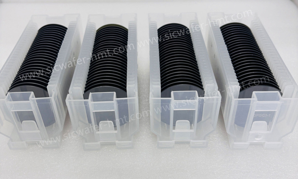
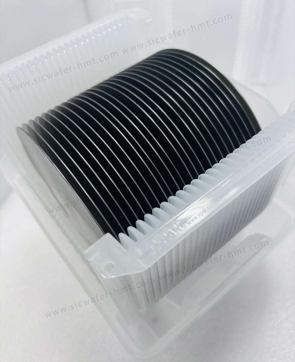
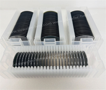
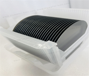
At HMT, we don't just supply SiC wafers – we engineer precision solutions for tomorrow’s technologies. While industry-standard As-cut SiC wafers typically measure 400μm, we empower your R&D and production with: Thickness Freedom: Break free from conventional limits with options ranging from 400μm to >1500μm – perfect for specialized applications requiring enhanced mechanical stability or ultra-thin profiles.
Full Diameter Spectrum: Seamlessly scale from prototyping to mass production with 2" to 8" wafer configurations.
Whether you’re pushing boundaries in EV power systems, next-gen 5G infrastructure, or quantum computing, our customizable as-cut SiC wafers are your blueprint for success.
| Parameter | HMT Standard | Custom Range |
|---|---|---|
| Diameter | 6" | 2"–8" |
| Thickness | 400μm | 500–1600μm |
| Resistivity | 0.015-0.028 Ω·cm | 0.015–0.025 Ω·cm |
| TTV | ≤15um | ≤10um |
Applications
Power ICs: SiC substrates for MOSFETs, Schottky diodes, and IGBTs.
RF Devices: High-frequency MMICs for 5G base stations and radar systems.
EV Components: Inverter-grade SiC wafers for automotive-grade power modules.
Quantum Computing: Ultra-low-loss SiC parts for cryogenic environments.
CATEGORIES
LATEST NEWS
- Introduction to the main functions of PbootCMS
Further Application of SiC Power Devices In New Energy Vehicles
- Introduction to the main functions of PbootCMS
SiC Wafer Manufacturer Production Analysis
- Introduction to the main functions of PbootCMS
Silicon Carbide SiC Wafer Polishing New Direction
- Introduction to the main functions of PbootCMS
SiC Boules and SiC Substrates industry chain
CONTACT US
Contact: Mr.Kimrui
Phone:
Tel: Please send your detailed inquiry or requirements via email below.
Email: kim@homray-material.com
Add: Please send your detailed inquiry or requirements via email below.