Silicon Carbide SiC Wafer Polishing New Direction
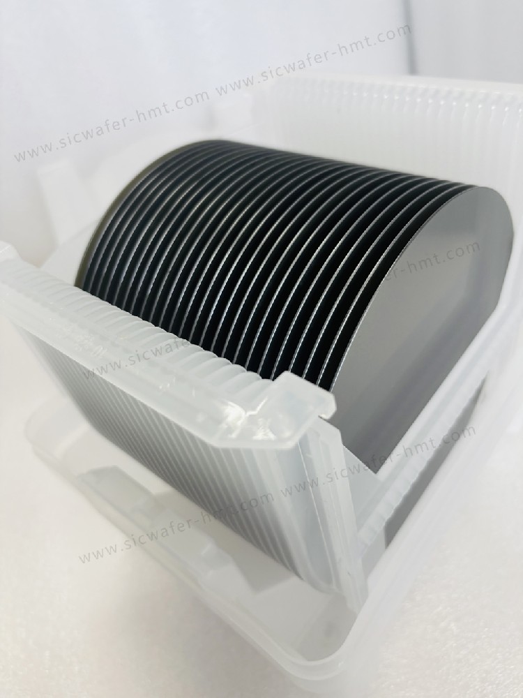
As a new semiconductor material, HMT offer 2 inch 4 inch 6 inch and 8 inch SiC wafers for Conductive N type and Semi-insulated HPSI type. SiC has the characteristics of high thermal conductivity, wide band gap, high breakdown electric field, high electron mobility, etc., making it one of the semiconductor materials with relatively concentrated research and development. Because of these properties, silicon carbide can be widely used in substrate, epitaxy, device design, wafer manufacturing and other fields.
 Sol-gel polishing technology is a green and efficient polishing method, through the use of semi-consolidated abrasives and flexible substrates, by virtue of the flexible characteristics of the soft matrix, the "tolerance" effect of the abrasive particles is achieved to achieve ultra-smooth and low defect density surface on the extremely hard semiconductor substrate. This method combines chemical and mechanical action to effectively polish extremely hard semiconductor substrates without causing severe surface or subsurface damage.
Compared with traditional CMP, sol-gel polishing technology can significantly reduce the surface roughness in a short time and achieve a higher material removal rate. Due to its good flexibility, the soft matrix can work under lower polishing pressure, reduce the pressure demand on the workpiece and equipment, reduce the wear and fall off of the wear particle, and extend the service life of the wear particle.
The precursor material (usually a metal-organic compound) is converted to sol, which forms a gel through hydrolysis and condensation reactions. In the sol-gel polishing pad, the wear particles are partially fixed in the gel matrix, which can provide a certain mechanical strength while maintaining the movement of the wear particles. Domestic scholars used this technology to process HTHP single crystal diamond (111) surface, polishing 22h, the surface roughness from 230nm to 1.3nm.

CATEGORIES
LATEST NEWS
- Introduction to the main functions of PbootCMS
Further Application of SiC Power Devices In New Energy Vehicles
- Introduction to the main functions of PbootCMS
SiC Wafer Manufacturer Production Analysis
- Introduction to the main functions of PbootCMS
Silicon Carbide SiC Wafer Polishing New Direction
- Introduction to the main functions of PbootCMS
SiC Boules and SiC Substrates industry chain
CONTACT US
Contact: Mr.Kimrui
Phone: 15366208370
Tel: 15366208370
Email: kim@homray-material.com
Add: LiSheng Industrial Building, 60SuLi Road, WuZhong District, JiangSu Province, P.R.China.