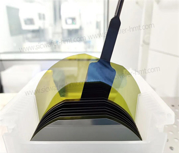
4 inch SiC Substrate Wafer Manufacturer
HMT supply both D grade and P grade 4 inch SiC substrate, 4 inch SiC Boules and 4 inch As cut SiC wafer without lapping or polishing.Are you looking f...
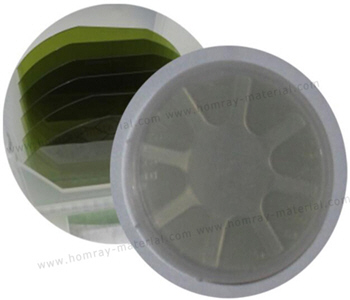
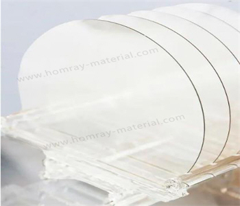
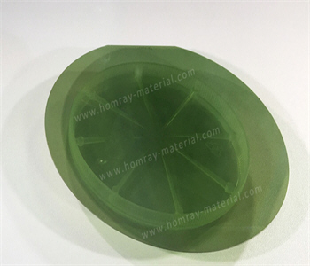
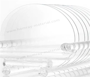
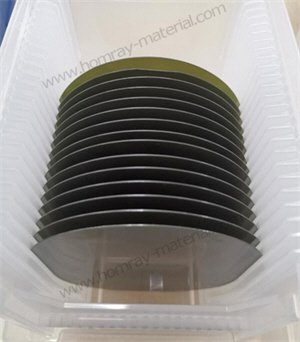
HMT supply both D grade and P grade 4 inch SiC substrate wafer, 4 inch SiC Boules and 4 inch As cut SiC wafer without lapping or polishing. Are you looking for 4 inch Conductive N type SiC wafer on the semiconductor market? Acutually, most SiC Wafer manufacturers stop production of 4 inch N type SiC Boule and 4 inch SiC Subtrate, because the mainstream is 6 inch SiC wafer/ SiC Boule and the newest 8 inch SiC substrate. But HMT still keep few 4 inch SiC Wafer capacity allocation for some our customers. If you have 4 inch SiC product demands ,please contact us and let us know your detailed spec of 4 inch SiC wafers.
4 inch As cut SiC Wafer 4 inch Polished SiC Substrate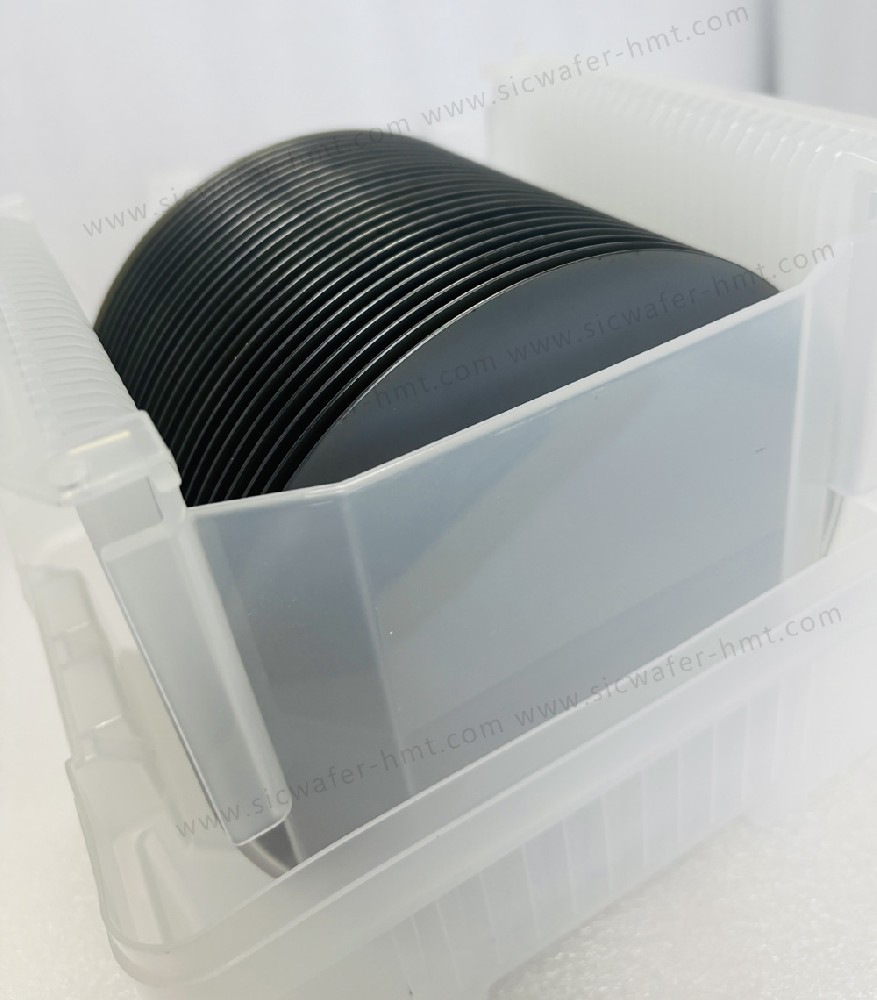
SiC has a higher power density than traditional silicon wafers, making the size and volume of devices smaller and the corresponding battery size smaller, thus extending battery life and giving electric cars longer range. Tesla's Model 3, for example, uses SiC instead of silicon for its current conversion module. The main form of SiC in semiconductors is as a substrate material. SiC substrate is the cornerstone of GaN and SiC applications in the third generation semiconductor materials. SiC materials mainly grow SiC epitaxial layer on conductive SiC substrate, which is used in all kinds of power devices. In recent years, with the maturity of technology and the decrease of preparation cost, the application of SiC in the field of new energy continues to penetrate.
Appications of SiC Wafer

CATEGORIES
LATEST NEWS
- Introduction to the main functions of PbootCMS
Further Application of SiC Power Devices In New Energy Vehicles
- Introduction to the main functions of PbootCMS
SiC Wafer Manufacturer Production Analysis
- Introduction to the main functions of PbootCMS
Silicon Carbide SiC Wafer Polishing New Direction
- Introduction to the main functions of PbootCMS
SiC Boules and SiC Substrates industry chain
CONTACT US
Contact: Mr.Kimrui
Phone: 15366208370
Tel: 15366208370
Email: kim@homray-material.com
Add: LiSheng Industrial Building, 60SuLi Road, WuZhong District, JiangSu Province, P.R.China.
