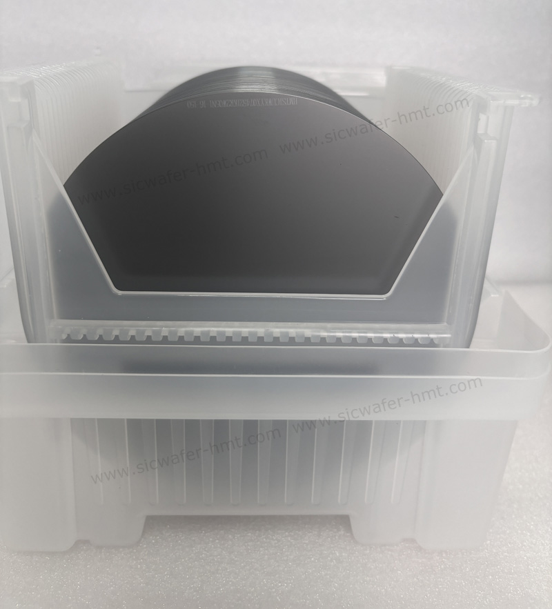
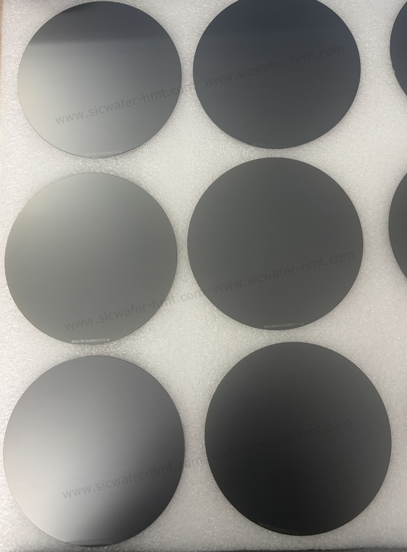
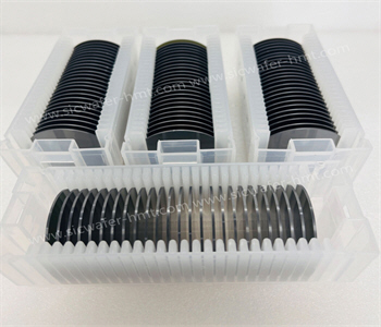
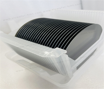
6 inch As Cut SiC Wafer Without lapping and polishing
HMT offer guaranteed 6 inch As Cut SiC Wafer Without lapping and polishing for grinding wheel, abrasives or newest polishing technology testing. The m...
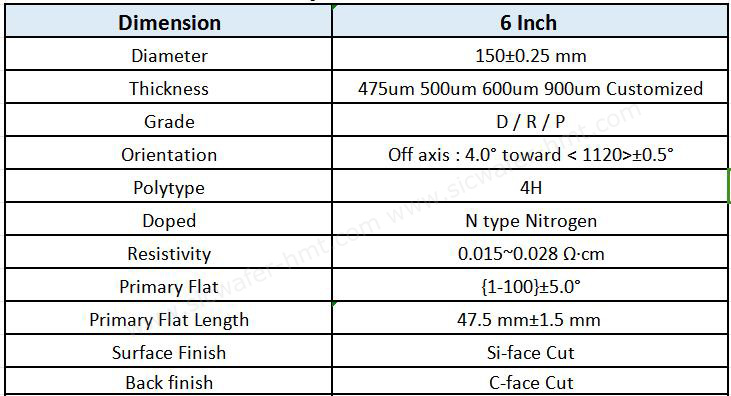
HMT offer guaranteed 6 inch As Cut SiC Wafer Without lapping and polishing for grinding wheel, abrasives or newest polishing technology testing. The mainstream is 6 inch un-polished raw SiC wafer in the market now. But HMT also supply the biggest and newest 8 inch without lapping and polishing SiC slicing wafers. Our leadtime of As-cut SiC wafer will be 3~5 weeks upon purchase quantity. Please feel free to contact us for without lapping raw SiC substrate parameters and quotation.
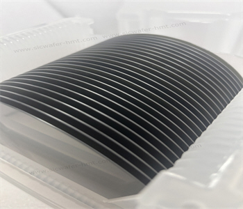
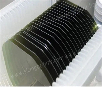
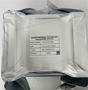
The package of 6 inch Raw Cut SiC wafer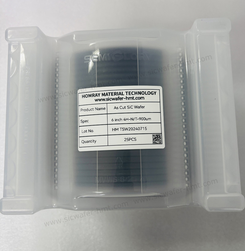
SiC device, the raw material for SiC, according to the different resistance properties, is divided into conductive SiC power devices and semi-insulated SiC based RF devices. The conductive SiC power device is mainly made by growing an epitaxial layer of SiC on a conductive substrate, and obtaining a SiC epitaxial sheet after further processing. Varieties include Schottky diodes, MOSFETs, IGBTs, etc., mainly used in electric vehicles, photovoltaic power generation, rail transit, data centers, charging and other infrastructure fields. The semi-insulated silicon carbon-based RF device is a gallium nitride epitaxial layer grown on the semi-insulated SiC substrate, and the silicon-based gallium nitride epitaxial sheet is prepared and further made, including HEMT gallium iso-nitride RF devices. It is mainly used in 5G communications, vehicle communications, national defense applications, data transmission, aerospace and other fields.
CATEGORIES
LATEST NEWS
- Introduction to the main functions of PbootCMS
Further Application of SiC Power Devices In New Energy Vehicles
- Introduction to the main functions of PbootCMS
SiC Wafer Manufacturer Production Analysis
- Introduction to the main functions of PbootCMS
Silicon Carbide SiC Wafer Polishing New Direction
- Introduction to the main functions of PbootCMS
SiC Boules and SiC Substrates industry chain
CONTACT US
Contact: Mr.Kimrui
Phone: 15366208370
Tel: 15366208370
Email: kim@homray-material.com
Add: LiSheng Industrial Building, 60SuLi Road, WuZhong District, JiangSu Province, P.R.China.
