SiC-on-SiC Epi Wafer
As the leading SiC Boules manufacturer and supplier, HMT also provide high quality 4 inch 6 inch 8 inch SiC Epitaxial on 4H-N substrate for the develo...
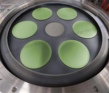
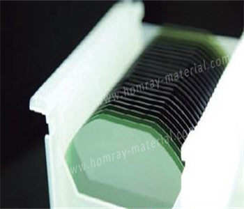
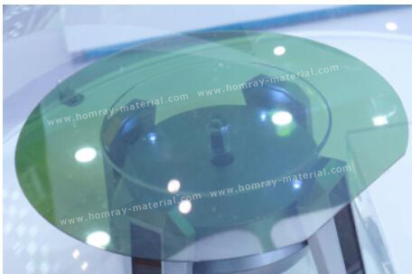
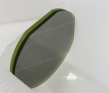
As the leading SiC Boules manufacturer and supplier, HMT also provide high quality 4 inch 6 inch 8 inch SiC Epitaxial on 4H-N substrate for the development of SiC devices. SiC on SiC Epi Wafer is mainly used for Schottky diodes, metal-oxide semiconductor field-effect transistors, junction field effect. Please contact us for more detailed SiC Epi Wafer spec. SiC substrate is divided into conductive N type substrate and semi-insulating SI substrate according to classification, the former of these two substrates is mainly used for the production of power devices, its epitaxial part is SiC, and the latter is mainly used for RF devices, its epitaxial is mainly GaN
In the field of medium and low pressure applications, SiC epitaxy technology is relatively mature. Basically, it can meet the needs of low and medium voltage SBD, JBS, MOS and other devices. The development of epitaxial technology in the field of high pressure is relatively lagging behind. At the same time, there are still many defects in the thick film required by high-voltage devices, especially triangular defects, which mainly affect the preparation of high-current devices. Large currents require large chip areas. And its minority lifetime is currently low.

CATEGORIES
LATEST NEWS
- Introduction to the main functions of PbootCMS
Further Application of SiC Power Devices In New Energy Vehicles
- Introduction to the main functions of PbootCMS
SiC Wafer Manufacturer Production Analysis
- Introduction to the main functions of PbootCMS
Silicon Carbide SiC Wafer Polishing New Direction
- Introduction to the main functions of PbootCMS
SiC Boules and SiC Substrates industry chain
CONTACT US
Contact: Mr.Kimrui
Phone: 15366208370
Tel: 15366208370
Email: kim@homray-material.com
Add: LiSheng Industrial Building, 60SuLi Road, WuZhong District, JiangSu Province, P.R.China.


