4H-SiC Wafer manufacturers
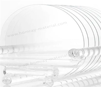
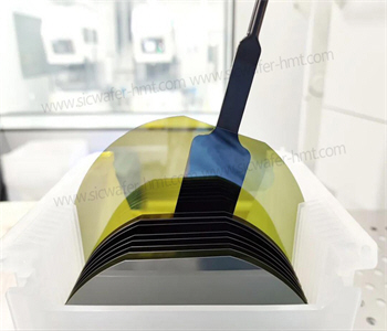
4H-SiC Wafer Manufacturers produce 2'' to 8'' on axis and off axis SiC Wafer with N type. Support customize wafer thickness and parameters with low co...
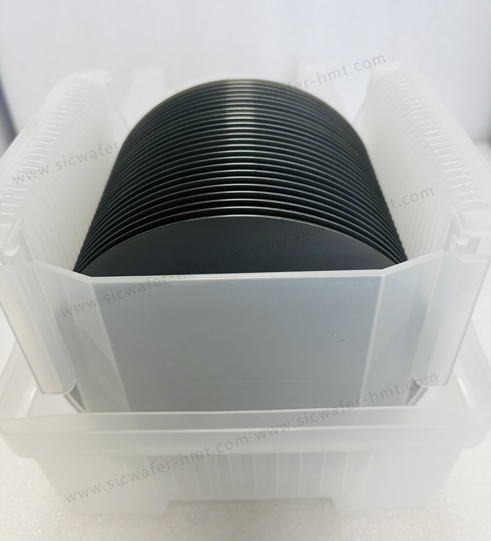
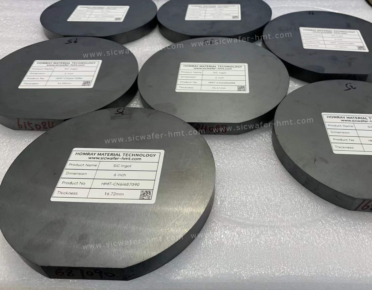
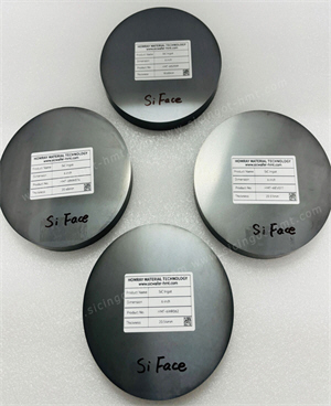
4H-SiC Wafer Manufacturers produce 2'' to 8'' on axis and off axis SiC Wafer with N type. Normally Conductive N type SiC Wafer orientation is off axis 4.0 toward<1120>±0.5° and Semi-insulated SI type wafer orientation is on axis <0001>±0.25°. We supply all grades of SiC Wafer based on different customers requirements and always providing preferential price. Meanwhile, we also offer all diameters (2 inch 4 inch 6 inch and 8inch) As cut SiC wafers without lapping and polishing and SiC Boules.
As-cut SiC Wafers SiC Boules
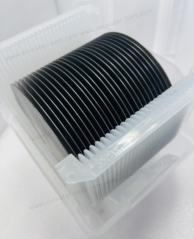
The advantages of 4H-N SiC Wafers as below:
1. High-temperature performance: SiC has high thermal conductivity and can operate at high temperatures, making it suitable for high-power and high-frequency electronic applications.
2. High breakdown voltage: SiC materials have a high breakdown voltage, enabling them to withstand high electric fields without electrical breakdown.
3. Chemical and environmental resistance: SiC is chemically resistant and can withstand harsh environmental conditions, making it suitable for use in challenging applications.
4. Reduced power loss: Compared to traditional silicon-based materials, SiC substrates enable more efficient power conversion and reduce power loss in electronic devices.
5. Wide bandgap: SiC has a wide bandgap, allowing the development of electronic devices that can operate at higher temperatures and higher power densities.
CATEGORIES
LATEST NEWS
- Introduction to the main functions of PbootCMS
Further Application of SiC Power Devices In New Energy Vehicles
- Introduction to the main functions of PbootCMS
SiC Wafer Manufacturer Production Analysis
- Introduction to the main functions of PbootCMS
Silicon Carbide SiC Wafer Polishing New Direction
- Introduction to the main functions of PbootCMS
SiC Boules and SiC Substrates industry chain
CONTACT US
Contact: Mr.Kimrui
Phone: 15366208370
Tel: 15366208370
Email: kim@homray-material.com
Add: LiSheng Industrial Building, 60SuLi Road, WuZhong District, JiangSu Province, P.R.China.

